


A reliable PCB relay assembly starts with five linked decisions: use the exact manufacturer footprint, preserve the required insulation distances, size the complete current path for heat, validate the solder process on the real board, and clean only when the relay construction and cleaning chemistry are compatible.
The most important rule is simple: do not copy a footprint, solder temperature, cleaning method or clearance value from a similar-looking relay. The plastic case may look familiar while the pin view, sealing construction, material system or thermal limit is different. Work from the exact orderable relay datasheet and the safety requirements of the finished equipment.
Engineering boundary: This guide supports PCB design and manufacturing planning. It does not replace the selected relay datasheet, the end-product safety standard, a formal insulation-coordination review or validation on the production PCB. Disconnect all coil and load power before inspection, rework or cleaning.
PCB Relay Layout, Soldering and Cleaning Checklist
|
Stage |
Decision to Lock |
Evidence to Keep |
|---|---|---|
|
Relay selection |
Exact model, coil, contact form, terminal style and protective construction. |
Approved part number and controlled datasheet revision. |
|
PCB layout |
Pin view, hole and pad dimensions, creepage, clearance, copper width, keep-outs and test access. |
Released footprint, insulation review and current-path calculation. |
|
Assembly |
Flux, preheat, soldering method, profile, cooling and handling. |
Profile records, first-article results and joint acceptance criteria. |
|
Cleaning and coating |
Whether cleaning is permitted, compatible chemistry, drying, venting and coating restrictions. |
Relay approval, chemical compatibility and process validation. |
|
Production release |
Electrical, thermal, insulation and contamination checks on representative assemblies. |
Qualified process window and traceable inspection plan. |
If any row is supported only by assumption, the assembly is not ready for production. A relay is part of a system: the component, PCB, solder joint, flux residue, coating, connector, enclosure, load and operating environment can all affect field reliability.
1. Start with the Exact Relay Footprint
Create the PCB library item from the drawing for the exact orderable relay. Check the manufacturer's view label carefully. A pattern marked bottom view is easy to mirror accidentally when it is transferred into a top-view CAD workflow. Confirm coil pins, common terminals, normally open contacts and normally closed contacts against the schematic before release.
Do not treat case dimensions as the footprint. The library also needs the specified hole diameter, pad geometry, terminal tolerance, component outline, courtyard, orientation mark and any manufacturer keep-out. For through-hole parts, distinguish the finished plated-hole size from the PCB fabricator's drill size. Plating reduces the final diameter, while an oversized finished hole can reduce support and solder control.
A useful footprint review asks four questions:
Electrical: Are the coil and every contact terminal mapped correctly?
Mechanical: Can the relay seat without forcing, terminal bending or case interference?
Manufacturing: Can flux, solder and cleaning processes be controlled around the body?
Inspection: Can operators or automated systems see the orientation mark, joints and relevant test points?
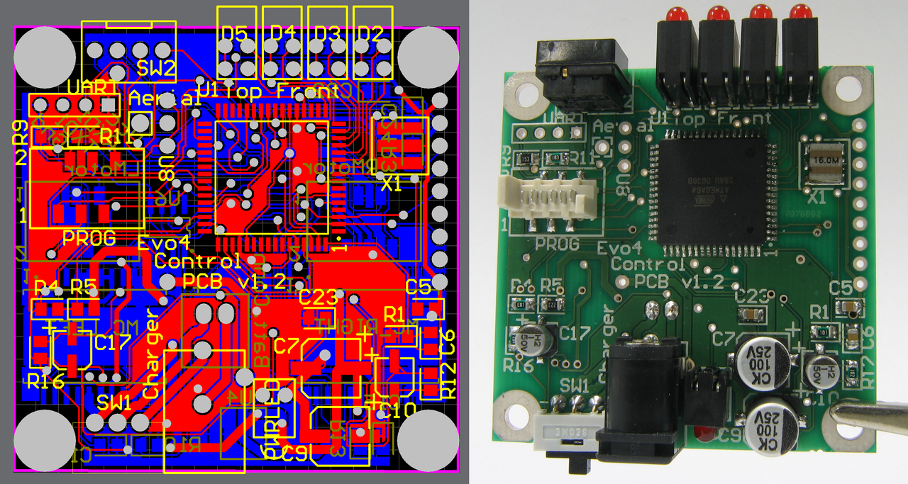
Image: PCB design and realisation by Mike1024, released into the public domain via Wikimedia Commons.
Before ordering a prototype, print the pattern at 1:1 scale or compare it with a verified mechanical sample. For high-risk assemblies, use CAD library approval that is independent from the person who created the footprint.
2. Set Creepage and Clearance from the End Application
Clearance is the shortest distance through air between conductive parts. Creepage is the shortest distance along an insulating surface. The correct values cannot be selected from relay contact voltage alone.
Insulation coordination may depend on the working voltage, transient overvoltage category, pollution degree, PCB material group or comparative tracking index, basic or reinforced insulation requirement, altitude and the standard that applies to the finished equipment. Slots, barriers, solder mask, coating and relay internal spacing do not all receive the same treatment in every standard.
|
Input |
Why It Matters |
Design Record |
|---|---|---|
|
Working voltage and waveform |
Establishes continuous electrical stress between circuits. |
Maximum RMS, peak and DC values at the relevant insulation barrier. |
|
Transient environment |
Affects the required impulse withstand and clearance. |
Overvoltage category, expected surge and protective devices. |
|
Pollution degree and material |
Surface contamination and tracking resistance affect creepage. |
Environment, controlled material group and board finish. |
|
Altitude |
Lower air density can require increased clearance. |
Maximum rated installation altitude and applied correction. |
|
Insulation function |
Functional, basic, supplementary and reinforced insulation have different purposes. |
Documented circuit boundary and applicable end-product clause. |
Measure the complete route, not only the space between relay pins. Copper pours, test pads, vias, mounting hardware, component leads and contamination-prone board edges can create a shorter path. Do not assume that solder mask automatically replaces the required creepage or clearance. If a routed slot is used, control its width, position, residue risk and fabrication tolerance.
IEC 60664-1 provides a framework for insulation coordination in low-voltage systems, while the finished product may impose additional rules. Record the selected values and their source so that a later footprint change cannot silently reduce the safety margin.
3. Design the Whole Contact Current Path for Heat
The relay contact rating does not prove that the PCB can carry the same current at an acceptable temperature. Copper traces, vias, pads, solder joints, connectors and local airflow form one thermal and electrical path. Their resistance produces heat according to P = I2R, so doubling current produces four times the resistive loss when resistance is unchanged.
Calculate trace width from the applicable PCB design method and the real copper thickness, allowable temperature rise, ambient temperature, board stack-up and duty cycle. Then check constrictions. A wide plane that narrows near the relay pad, a small annular ring, insufficient via area or a connector pin can become the hottest point.
Keep high-current paths short where practical. Use symmetric copper where parallel contact paths are intentionally designed, and do not assume parallel relay poles share current equally unless the relay manufacturer permits that use and the system has been validated. Contact timing and path resistance can concentrate current in one pole.
For a power relay prototype, measure temperature at the relay terminals, contact-side copper, nearby connector and enclosure hot spot. Test at maximum expected load, worst-case ambient, realistic airflow and the highest credible coil duty. A room-temperature bench test with an open enclosure can hide the production risk.
4. Separate Coil/Control and Contact/Load Zones
The relay provides galvanic separation only when the PCB preserves it. Route low-voltage coil drive and sensitive signals on the control side. Route the switched load on the contact side. Avoid crossing a safety isolation boundary on another layer with copper, test points or unrelated components.
Place the coil driver, flyback or other suppression component close to the coil loop when appropriate. A suppression choice is not only an EMC decision: it can change relay release time and therefore contact behavior. A simple diode across a DC coil can reduce the voltage spike but may slow release. Select suppression with the relay manufacturer's guidance and the required switching behavior.
High di/dt contact loops and long load traces can couple noise into coil control, sensing and communication circuits. Keep sensitive traces away from relay contact routing, control return current intentionally and review the location of connector shields and protective earth. If the load produces severe transients, coordinate contact-side suppression with the load, safety requirements and expected relay life.
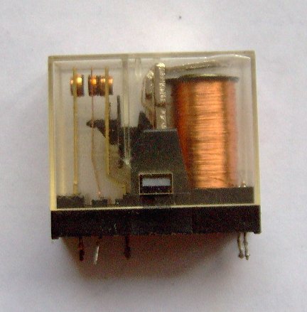
Image: Electronic component relay by FDominec, licensed under CC BY-SA 3.0 via Wikimedia Commons.
5. Match the Soldering Process to the Relay Type
Most PCB power relays use through-hole terminals and may be assembled by wave soldering, selective soldering or hand soldering. Surface-mount relays use a specified reflow profile. The correct process depends on the exact relay construction and datasheet.
|
Method |
Main Controls |
Typical Risk |
|---|---|---|
|
Wave soldering |
Flux height, preheat, wave contact, solder level, conveyor speed and cooling. |
Flux or solder entering a non-sealed relay; excessive thermal exposure. |
|
Selective soldering |
Nozzle program, dwell, board support, local flux and adjacent-part exposure. |
Repeated local heating or poor fill on high-thermal-mass joints. |
|
Hand soldering |
Controlled tip condition, temperature, contact time, solder feed and operator technique. |
Long dwell, pad damage, excess flux or mechanical stress during rework. |
|
SMT reflow |
Manufacturer profile, ramp, soak, peak, time above liquidus and cooling. |
Case or seal damage when a non-SMT relay or invalid profile is used. |
Do not transfer a temperature limit from another manufacturer or model. Even a published general guideline may say "unless otherwise specified." The model datasheet takes priority, and the actual board must still be evaluated because a thick multilayer PCB or large copper plane changes heating and wetting.
IPC J-STD-001 defines process and material requirements for soldered electrical and electronic assemblies, while IPC-A-610 addresses post-assembly acceptability. Product class, customer requirements and the latest controlled revisions should be established before production.
6. Control Flux, Preheat, Solder Exposure and Cooling
Flux Application
Use a qualified, non-corrosive flux system that is compatible with the assembly process. Prevent flux from rising above the PCB and entering the relay. This is especially important for open, dust-cover and flux-resistant constructions. Applying excessive flux is not a reliable cure for poor solderability; it can move contamination into places that inspection cannot see.
Preheat
Preheat can improve solderability, reduce thermal shock and help limit flux penetration during automatic soldering. The permitted condition is model-dependent. Verify board-side temperature rather than relying only on machine setpoints, and include the thermal mass of the final PCB.
Solder Exposure
Keep solder temperature and contact time within the exact relay requirement and the qualified assembly window. The joint must achieve proper wetting without exposing the relay, pad or laminate to excessive heat. When the board contains large copper areas, use process development rather than simply increasing time until the hole fills.
Cooling and Handling
Stabilize the assembly after soldering. Manufacturer guidance commonly warns against placing a hot sealed relay immediately into cold cleaning liquid because thermal shock can damage sealing performance. Do not bend terminals to make an ordinary relay self-clinching, and do not push or straighten the case while joints are cooling.

Image: Soldering-PCB-b by Tlapicka, licensed under CC BY-SA 3.0 via Wikimedia Commons.
7. Know the Relay Protective Construction Before Cleaning
Words such as dust cover, flux resistant, plastic sealed, washable and hermetically sealed are not interchangeable. The exact manufacturer definition controls what the relay can tolerate during soldering, cleaning and operation.
|
Construction |
Process Assumption to Avoid |
Required Action |
|---|---|---|
|
Open or dust-cover relay |
Assuming the cover makes the component washable. |
Prevent flux and cleaning liquid entry; follow exact restrictions. |
|
Flux-resistant relay |
Assuming resistance to solder flux means immersion cleaning is allowed. |
Use only the solder and cleaning processes approved for the model. |
|
Plastic-sealed or washable relay |
Assuming every solvent, ultrasonic process or thermal shock is safe. |
Confirm chemistry, method, time, temperature, drying and venting instructions. |
|
Hermetically sealed relay |
Assuming the external package removes all board-process risks. |
Follow the specific package, terminal and cleaning requirements. |
Verify the suffix in the ordered part number. One relay family may offer multiple protective versions with different process permissions. Receiving inspection should confirm that the delivered suffix matches the approved manufacturing flow.
8. Use a Cleaning Decision Workflow
Cleaning should solve a defined contamination or electrical-reliability problem. It should not be an automatic step applied to every relay assembly. Follow this sequence:
Step 1: Identify the exact relay construction. Obtain the model datasheet and manufacturer processing guidance. If washability is unclear, treat the relay as not approved for immersion until the supplier confirms it.
Step 2: Define why cleaning is needed. Examples include ionic residue limits, high-impedance circuitry, coating adhesion or customer cleanliness requirements. If a validated no-clean process meets the assembly requirement, unnecessary washing may add risk.
Step 3: Qualify the chemistry and method. Check compatibility with the relay case, seal, label, PCB laminate, solder mask, connector plastics and coating system. Spray, brush, immersion, vapor and ultrasonic processes do not create the same exposure.
Step 4: Control temperature and mechanical energy. Avoid rapid hot-to-cold transfer. Do not use ultrasonic cleaning unless the exact relay is approved for it; relay manufacturers warn that ultrasonic energy can contribute to coil damage or contact sticking in unsuitable products.
Step 5: Rinse, dry and vent as specified. Trapped moisture or contaminated solvent can move residue rather than remove it. Some washable relays with a manufacturer-provided vent require opening after processing and before electrical operation. Follow the exact product instruction.
Step 6: Validate after cleaning. Inspect residues and case damage, then verify insulation, contact behavior and coil operation on representative samples. Include aged or stressed samples when the application consequence justifies it.
9. Check Conformal Coating and Potting Compatibility
Conformal coating can protect the PCB, but it can also enter a non-sealed relay, attack the plastic case or seal, change heat flow and place stress on solder joints. Do not coat over a relay unless the exact combination of relay construction, coating chemistry and process has been approved.
Keep coating away from vents and other manufacturer-designated openings. If the relay must be installed after coating, protect the solderable area and confirm that the secondary soldering process remains controlled. If masking is used, verify that removal does not pull the case, terminals or cured coating.
Silicone-containing materials deserve special attention around electromechanical contacts. Volatile silicone compounds can contribute to contact problems under electrical switching conditions. Review not only the coating but also sealants, adhesives, gaskets, lubricants and nearby processes.
Potting the entire relay can change heat dissipation, mechanical stress and acoustic behavior. Treat it as a new application condition requiring manufacturer review and representative testing.
10. Validate the Process on the Production PCB
A process is not qualified because one relay survived one solder cycle. Validate the full manufacturing window on the actual PCB, including the thickest copper, highest thermal mass, expected machine variation, approved flux quantity, cleaning exposure and rework limit.
|
Validation Area |
What to Check |
Typical Evidence |
|---|---|---|
|
Footprint and assembly |
Orientation, seating, hole fit, pad integrity and case clearance. |
First-article inspection and dimension report. |
|
Solder process |
Board temperature, exposure time, fill, wetting, voiding where relevant and rework. |
Thermocouple profile, inspection record and cross-section if needed. |
|
Cleanliness |
Residue, solvent entrapment, drying, visible case attack and coating adhesion. |
Qualified cleanliness method and visual/electrical results. |
|
Electrical function |
Coil operation, pickup/release behavior, contact continuity and insulation. |
End-of-line limits and sample qualification results. |
|
Thermal performance |
Terminal, copper, connector and enclosure temperature at worst-case duty. |
Thermal test report with load, ambient and airflow recorded. |
Define reactions for out-of-window conditions. If the solder pot temperature, conveyor speed, cleaning concentration or drying time leaves the qualified range, operators need a controlled hold-and-review process rather than an informal visual check.
11. Common Failures and What They Suggest
|
Observed Problem |
Possible Process Cause |
Next Check |
|---|---|---|
|
Relay does not operate after assembly |
Wrong footprint orientation, coil damage, terminal stress or incorrect coil version. |
Part number, pin map, coil resistance, drive voltage and assembly history. |
|
Intermittent or high contact resistance |
Flux, cleaner, coating vapor or other contamination reached the contacts. |
Protective construction, chemical process, residue path and contact load. |
|
Hot PCB around the relay |
Trace constriction, weak solder joint, undersized via field, connector loss or excessive load. |
Current waveform, voltage drop and temperature along the full path. |
|
Solder crack after mechanical or thermal cycling |
Board flex, forced terminal fit, insufficient support or coating/potting stress. |
Hole tolerance, case seating, board support and strain sources. |
|
Insulation test failure |
Insufficient spacing, residue, moisture, conductive debris or damaged coating. |
Shortest board path, cleanliness, drying and end-product insulation requirement. |
|
Case or seal damage |
Excessive solder heat, incompatible solvent, thermal shock or ultrasonic exposure. |
Profile record, chemical compatibility and process sequence. |
Do not diagnose every post-assembly failure as a defective relay. Preserve failed samples and process records. Compare unassembled components, assembled-but-not-cleaned boards and fully processed boards to locate when the change occurred.
12. Information to Send a Relay Supplier
A supplier can give better guidance when the request describes the actual assembly instead of asking only for a current rating. Include:
Relay requirement: coil voltage and tolerance, AC or DC coil, contact form, load voltage, load current, load type, switching rate, expected life and protective construction.
PCB information: board thickness, copper weight, hole and pad proposal, maximum ambient, enclosure, airflow, isolation requirement and maximum altitude.
Assembly process: wave, selective, hand or reflow soldering; lead-free alloy; flux type; preheat; proposed time and temperature; cleaning method; cleaning chemistry; drying; coating and potting.
Compliance: target market, end-product standard, insulation class, required certifications and any customer workmanship class.
You can review the QIANJI PCB relay range to identify a suitable family. For example, the QIANJI JQX-14F datasheet includes its own dimensions and bottom-view pattern; those details belong to that model and should not be copied to another relay. For help matching a relay and assembly process, send QIANJI your application details.
Frequently Asked Questions
Can I use the footprint from a relay with the same case size?
No. Verify the exact model drawing. Pin spacing, contact form, view orientation, terminal size and tolerance can differ even when two cases look similar.
What creepage and clearance should I use around a PCB relay?
There is no universal value. Determine it from the finished equipment's insulation requirements, working voltage, transient environment, pollution degree, PCB material, altitude and applicable standard. Check the shortest path across the whole PCB.
Can a dust-cover or flux-resistant relay be immersion cleaned?
Do not assume so. Flux resistance and washability are different properties. Manufacturer guidance from Panasonic and TE explicitly distinguishes non-washable open or dust-cover constructions from plastic-sealed products approved for specified cleaning.
Is ultrasonic cleaning safe for a sealed relay?
Only if the exact relay manufacturer approves it. Panasonic and Omron warn that ultrasonic energy can damage unsuitable relays, including coil or contact mechanisms. A sealed case by itself is not approval for ultrasonic cleaning.
Can I use a general relay soldering temperature from an online guide?
Use the exact model limit and validate it on the real board. General manufacturer pages often include default conditions, but they also state that model-specific requirements and actual production conditions take priority.
Does a plastic-sealed relay remain sealed after cleaning?
Follow the exact product instruction. Some washable relays have a tape seal or vent nib that must be opened after board processing and before operation. Do not vent a relay unless its manufacturer requires that action for the selected model.
Should relay pins be cut after soldering?
Avoid terminal cutting unless the manufacturer and assembly design allow it. Cutting can transmit vibration or mechanical force into the relay and joint. Use the correct terminal length and board stack-up from the start.
What should be tested before mass production?
At minimum, verify footprint and orientation, solder profile and joint quality, cleanliness, drying, coating compatibility, coil/contact function, insulation and worst-case thermal performance. Add environmental and life testing according to application risk.
Final Design Rule
A PCB relay is reliable when the component specification and board process agree. Lock the exact part number, preserve the required isolation, remove current-path hot spots, qualify the solder profile, and make cleaning and coating conditional on the relay's protective construction.
If the process requires a condition that the relay documentation does not clearly permit, stop and obtain written guidance or choose a construction designed for that process. That decision is usually less expensive than diagnosing contamination, cracked joints, insulation failures or damaged seals after production.
Technical References
This guide was cross-checked against the following primary technical sources:
1. IEC 61810-1:2015, Electromechanical elementary relays – General and safety requirements.
2. IEC 60664-1:2020/AMD1:2025, Insulation coordination for equipment within low-voltage supply systems.
3. IPC announcement for J-STD-001J and IPC-A-610J.
4. Panasonic Relay Soldering and Cleaning Guidelines.
5. Omron Safety Precautions for Relays.
6. TE Connectivity: Mounting, Termination and Cleaning of PCB Relays.